
Electron Beam Melting (EBM)
In a vacuum (protection against oxidation), conductive metal powder is melted with an electron beam. The electrons are directed via a magnetic field and three-dimensional components are produced layer by layer in the heated powder bed. The process-related pre- and post-heating avoids or minimizes thermal stresses. This process is therefore suitable for processing materials that are prone to cracking, such as tungsten.
Innovative 3D printing of divertor parts made of tungsten for the FUSION program
The divertor is the component of the fusion reactor that has to withstand the highest thermal loads. The current EUROfusion DEMO baseline assumes 10 MW/m² in a stationary state and up to 20 MW/m² for transients of a few seconds. Only tungsten or tungsten-based alloys can be considered as shielding materials, while a copper base is assumed for the heat sink, i.e. the pipe for the coolant. KIT is pursuing a new approach with the additive manufacturing of the W-shielding and the connecting structure as well as the infiltration with the copper for the heat sink. In this way, a form-fit between the shield and heat sink can be achieved even with flat shield geometries, which can otherwise only be realized by complex welding of monoblock shield geometries that enclose the heat sink.
In 2023, tungsten divertor parts of various geometries were successfully printed three-dimensionally using electron beam melting (EBM). A small prototype ("mock-up") was successfully tested in the Garching LArge DIvertor Sample Test Facility (GLADIS) at IPP Garching for high heat fluxes (100 pulses of 20 s with up to 20 MW/m²). During the cyclic load with 20 MW/m², the surface temperature of the W-EBM flat roof tiles rose to up to 2520 °C. After the test, no macroscopic failures, damage or cracks were detected on the tungsten flat tiles. These promising results form the basis for the production of the next series of models with optimized designs and cooling channels made of CuCrZr, which is more temperature-resistant than copper.
 |
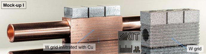 |
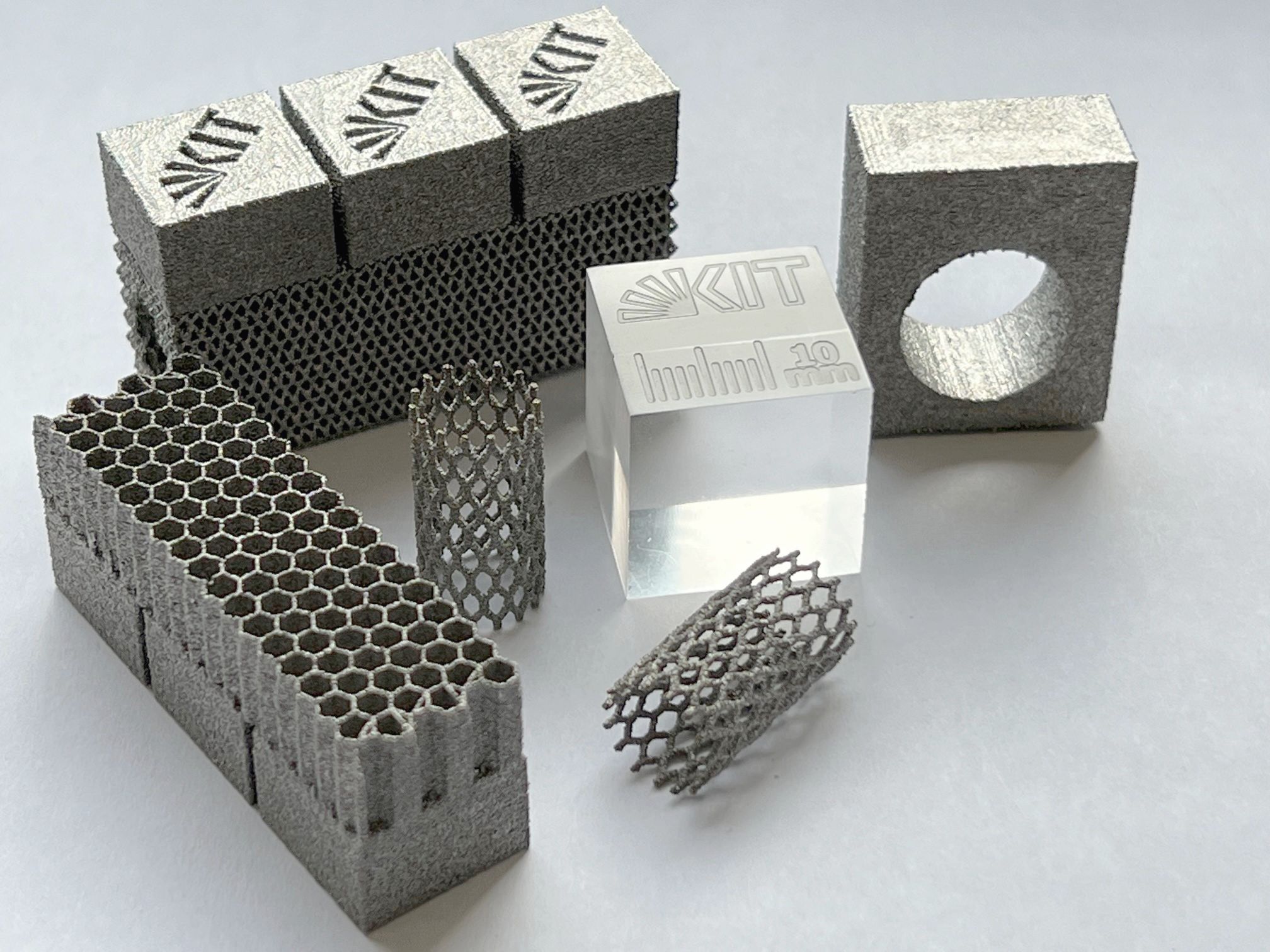
The image on the left shows various tungsten samples that were printed three-dimensionally using electron beam melting (EBM). The image on the right demonstrates the path from the printed component to the final test structure after infiltration with copper.
A second research approach is the combination of electron beam melting with selective laser melting (SLM). The components were first manufactured from tungsten using EBM, then placed in a laser system and the copper powder melted using a laser in order to additively manufacture the copper cooling channels.
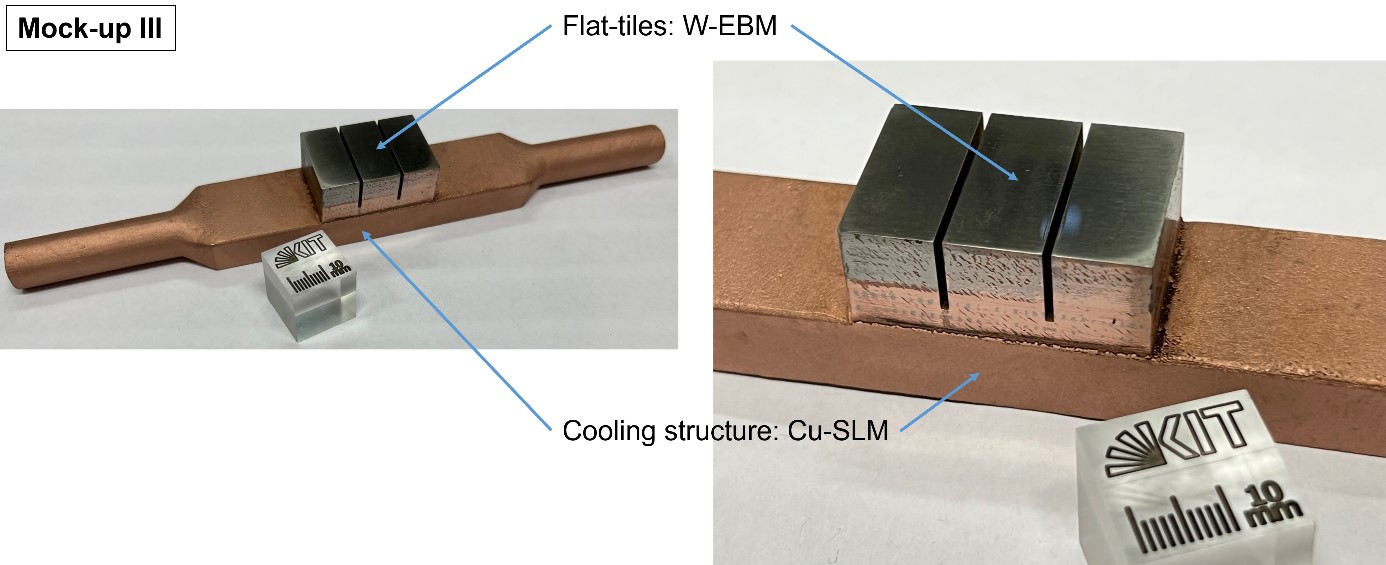 |
The picture shows the final prototype which was produced using a combination of two additive manufacturing processes (W-EBM and Cu-SLM).
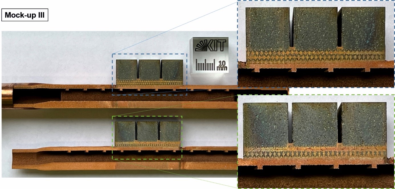 |
The illustration shows the analysis of the additively manufactured prototype after the heat flow test
Publikation
Guth, S.; Babinský, T.; Antusch, S.; Klein, A.; Kuntz, D.; Šulák, I.
2026. International Journal of Fatigue, 202, Art.-Nr.: 109238. doi:10.1016/j.ijfatigue.2025.109238